General-purpose printing equipment

ULTRA-HIGH PRECISION ADDITIVE MANUFACTURINCSOLUTIONS FOR ELECTRONICS

EP100/EL400/EP400/EP600

Combining micro-nano Direct Ink Writing (DIW) additive printing technology with proprietary nanoscale inks, this system delivers 3D printing at feature sizes of 1–10 μm.

  • Minimum feature size down to 1 μm
  • Extensive material library for diverse printing scenarios
  • Capable of printing complex 2D and 3D structures
  • High pattern clarity and excellent line morphology consistency
  • Quick-release print head for fast and convenient swapping
  • 100% material utilization rate

UNIVERSAL 5-AXIS ELECTRONIC ADDITIVE MANUFACTURING PLATFORM

EP600-FP-5X

This platform integrates a high-precision five-axis motion system with direct writing technology, enabling precise deposition of conductive, insulating, encapsulating, and other functional materials onto complex curved substrates.

  • Minimum line width of 60 μm on curved surfaces
  • Supports precise distribution of diverse inks/materials

  • Simplified tool path generation via direct CAD import

  • Available in simultaneous or 3+2 positional versions

  • Working area of 180 × 180 × 90 mm

  • Designed for R&D and prototyping applications

ULTRA-HIGH PRECISION FLUID DISPENSER

EP600-FD

Utilizes pneumatic direct writing technology combined with a self-developed dispensing printhead module to achieve precision dispensing of epoxy, silicone, UV adhesives, and more.

  • Supports dispensing on substrates and wafers
  • Supports CAD pattern import for processing

  • Self-developed adjustable array dispensing module

  • Self-developed tilt-and-rotate dispensing module

  • Equipped with an in-situ UV curing module

  • Supports a maximum processing area of 12 inches

ULTRA-HIGH PRECISION VIA FILLING 3D PRINTERT

EP400-FH / EP600-FH

Direct Ink Writing (DIW) additive printing technology combined with micro-nano conductive metal pastes enables metallization of precision interconnect vias such as TSV, TGV, and TMV.

  • Eliminate the need for pre-deposited seed layers
  • Environmentally friendly process (without electroplating)

  • Supports direct CAD drawing import for fully automated machining

  • Precision micro-holes support blind-hole filling

  • High-solid-content materials have high packing density

  • Filling materials can be cured at temperatures below 200℃

MICRO-DIW METAL 3D PRINTER

EP600-ES

Utilizes micro‑nano Direct Ink Writing (DIW) additive printing technology combined with a self‑developed adjustable array multi‑printhead module to fabricate conductive 3D structures (vertical walls, pillars) for applications such as electromagnetic shielding of RF modules and interconnects in stacked packaging.

  • Supports in-situ printing of conductive three-dimensional microstructures
  • Supports standard carrier board and 12-inch wafer processing

  • Features adaptive process closed‑loop parameter tuning

  • Self-developed high three-dimensional forming performance conductive paste

  • Self-developed adjustable array parallel printing module

  • Filler material curing temperature below 200°C

MULTIFUNCTIONAL SOLDER PASTE PRINTER

EP400-SP

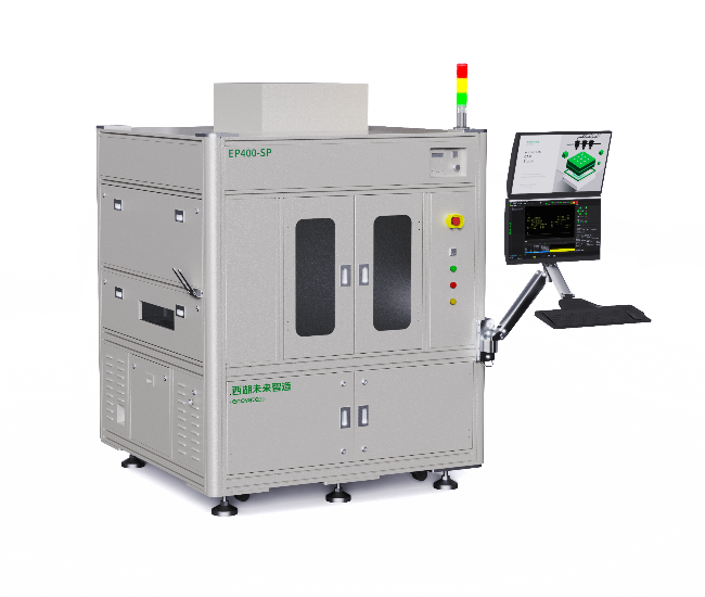
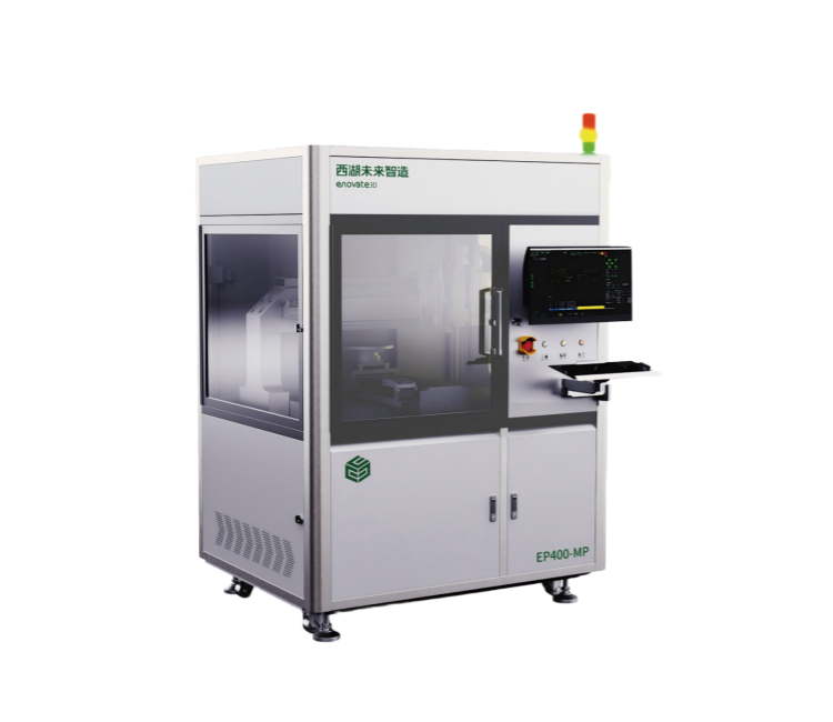
Combines high-speed jetting technology with direct writing dispensing technology to achieve precise solder paste printing and micro-dispensing. The minimum jetting spot diameter can be as small as 250 μm, and the minimum dispensing diameter can be as small as 100 μm. Suitable for deep‑cavity packages, flexible substrates, and similar products.

  • Adjustable rail supports a maximum width of 350 mm
  • Minimum solder paste jetting spot diameter down to 250 μm

  • Supports Gerber file import for automated processing

  • High motion acceleration ensures processing efficiency

  • Supports deep-cavity products of 6 mm and above

  • Compatible with a variety of solder pastes such as SAC305, SnPb, and more

MOLTEN METAL PRINTER

EP400-MP

Utilizes a self-developed fused direct writing valve to heat, melt, and pattern-print alloy solders such as InAg, SnBi, SAC305, and SnSb, suitable for MEMS and hermetic packaging solder bonding.

  • Supports pattern printing of alloy solders
  • Supports wafer map file import

  • Supports melt printing of commonly used solders

  • Supports localized inert gas atmosphere for oxidation prevention

  • Typical printing feature size: 150 μm

  • Supports a maximum processing area of 8 inches

  • Supports multiple modes including line drawing and dot dispensing